


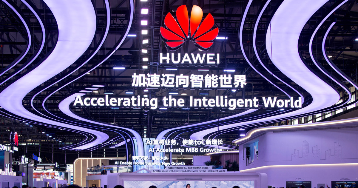
SHANGHAI—Chinese technology giant Huawei announced Monday that it has achieved a breakthrough that will allow it to produce cutting-edge chips within five years, touting the news as a major milestone in Beijing’s efforts to circumvent U.S. technology regulations.
Subscribe to read this story without ads
Get unlimited access to ad-free articles and exclusive content.

U.S. sanctions that began in 2019 have largely cut Huawei off as a global maker of semiconductor chips, the tiny brains that power everything from smartphones to computers to cars, as the U.S. and China battle for global dominance in artificial intelligence.
The U.S. government has also restricted the Chinese government’s access to chip design software and semiconductor manufacturing equipment, such as lithography machines, which has led the Chinese government to invest billions of dollars in developing its own semiconductor supply chain.
Huawei announced Monday at a technology conference in Shanghai that by 2031, its high-end chips will have transistor densities comparable to the 1.4-nanometer process considered the industry’s most advanced.
This compares to the 7-nanometer, currently considered China’s most advanced chip manufacturing capability, and the 2-nanometer manufacturing technology used by Taiwan-based TSMC, the world’s leading manufacturer of advanced chips. TSMC, which makes chips for American technology giant Nvidia, said it plans to begin mass production using the 1.4-nanometer process in 2028.

forsubscriber

US tech CEOs join Trump in China
01:24
He Tingbo, president of Huawei’s semiconductor business, said in a speech that Huawei has devised a breakthrough “LogicFolding” design for future Kirin chips. This means that rather than achieving performance gains by shrinking transistors (a process that requires extreme ultraviolet lithography machines that China doesn’t have access to), Huawei is folding traditional 2D circuits into 3D vertical skyscrapers, essentially stacking chips on top of each other.
Huawei also announced a new principle called tau scaling on Monday, although it did not provide any independent performance data to back up its announcement. This focuses on folding and stacking the chips to reduce the time it takes for data to move through the chip.
This is a departure from Moore’s Law, which has long guided the industry with the idea of packing more transistors into smaller chips, but is widely seen as reaching its limits.
“The industry will face these problems sooner or later,” Ms. He, known in China’s high-tech industry as Huawei’s “chip queen,” told reporters through an interpreter after her speech. “We are confident in this path because practice has proven it.”
The new methodology is not without its challenges, he said. He said traditional tools are still not good enough for full-scale free logic designs, and with components stacked vertically, thermal management remains a key issue.
“Cost, power, heat and system integration remain major challenges” for Chinese technology, said Brady Wang, an associate director and analyst at Counterpoint Research.
“In the short term, China may close the gap with world leaders, but the technology gap with the most advanced nodes will remain,” he told Reuters.
But a paradigm shift from Moore’s Law to Tau Scaling (dubbed “Her Law” after him) could help Huawei avoid a shortage of lithography equipment and bring it one step closer to independence in the global chip race.
On the Chinese social media platform Weibo, the hashtag #HuaweiSemiconductorFieldNewBreakthrough has been viewed 40 million times, and that number continues to grow.
Some commenters referred to an AI model released last year by a Chinese startup that they described as a “deep-seek moment” for the Chinese chip industry, which was said to perform as well as or better than leading U.S. models at a fraction of the cost.
Some believe that US sanctions have encouraged Chinese innovation.
“The more sanctions from the West, the more China will advance!” one Weibo user wrote.
After Huawei was forced into “survival mode” due to U.S. regulations, it made a comeback in 2023 with the launch of its Mate 60 series of smartphones, but its surprisingly advanced Chinese-made 5G chips raised questions about whether the regulations were still working.
Last September, Huawei announced a three-year roadmap for AI chip development, effectively filling the hole left by Nvidia’s exclusion from the Chinese market. The Trump administration said late last year that Nvidia might sell its powerful H200 chips to certain Chinese companies, but no orders have been placed yet.
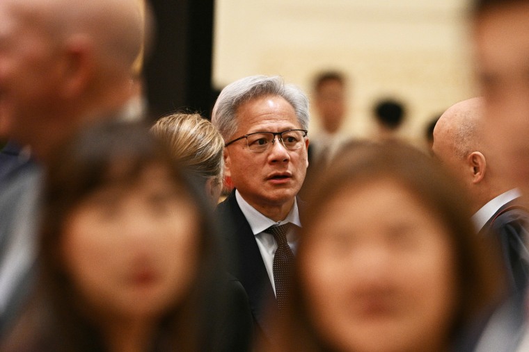
Nvidia CEO Jensen Huang, who traveled to China this month with President Donald Trump for a summit with Chinese leader Xi Jinping, told CNBC last week that the company had “significantly conceded” China’s chip market to Huawei.
But on Saturday, he signaled that the Chinese market remains an important source of long-term demand, telling reporters in Taiwan that China is part of the $200 billion market he expected for Nvidia’s new Vera central processing unit.
Chinese state media insisted after Huawei’s announcement on Monday that the United States and China should find ways to cooperate as much as possible.
“China does not deny the existence of competition, but such competition must be moderate and healthy, with the aim of mutual progress rather than a zero-sum game,” read a commentary posted on social media accounts associated with Chinese state broadcaster CCTV.
Last week, a Chinese Foreign Ministry spokesperson announced that Trump and Xi agreed to start an intergovernmental dialogue on AI at their Beijing summit.
“The United States and China should work together to promote the development and governance of AI,” Guo Jiakun told reporters, “so that AI can better contribute to the progress of human civilization.”
Janis Mackey Frayer and Dawn Liu reported from Shanghai and Jennifer Jett from Hong Kong.
